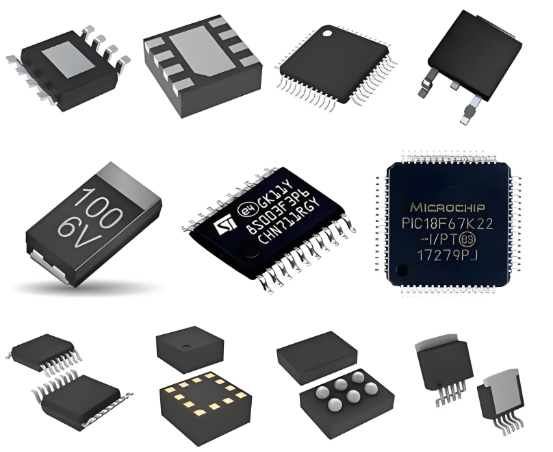
Lattice LCMXO2-7000HE-4TG144I: A Comprehensive Technical Overview of Low-Power FPGA Capabilities
The Lattice Semiconductor MachXO2™ series represents a significant leap in low-power, low-cost programmable logic solutions, with the LCMXO2-7000HE-4TG144I standing out as a powerful embodiment of these capabilities. This FPGA, packaged in a compact 144-pin TQFP, is engineered for a wide array of applications, including consumer electronics, industrial control systems, telecommunications infrastructure, and general-purpose logic integration. Its architecture is meticulously designed to deliver a unique blend of high functionality and remarkably low power consumption, making it an ideal choice for modern, power-sensitive designs.
At the core of the LCMXO2-7000HE-4TG144I is its non-volatile, flash-based technology. This foundational feature eliminates the need for an external boot PROM, streamlining board design and enhancing overall system security. Upon power-up, the device configures itself instantaneously, leading to faster system start-up times and a more reliable state-machine operation compared to SRAM-based FPGAs.
The device boasts a substantial logic capacity of 6864 Look-Up Tables (LUTs), providing ample resources for implementing complex combinatorial and sequential logic. This is complemented by 240 Kbits of embedded block RAM (EBR), which serves as efficient on-chip memory for data buffering, FIFOs, and state storage, reducing the need for external memory components and further minimizing the system's footprint and power budget.

A key strength of the MachXO2 family is its ultra-low static power consumption, often measured in microamps (µA). This is critical for battery-operated and always-on applications where every microwatt counts. The device supports multiple low-power modes, allowing designers to finely tune power usage based on performance requirements. Furthermore, it features programmable I/O capabilities supporting a wide range of voltages (e.g., 1.2V, 1.5V, 1.8V, 2.5V, 3.3V LVCMOS), ensuring seamless interface with other components in a mixed-voltage environment.
Beyond generic logic, the LCMXO2-7000HE integrates dedicated hard intellectual property (IP) blocks. It includes a User Flash Memory (UFM) block, which offers up to 256 Kbits of additional non-volatile storage for user data, boot code, or system configuration parameters. Most notably, it incorporates a hardened I2C, SPI, and Timer/Counter block. This pre-engineered logic accelerates the implementation of common serial communication interfaces and timing functions, saving valuable logic resources and reducing design time.
The device is supported by Lattice's robust ispLEVER® Classic Design Suite and the newer Lattice Radiant® software. These development environments provide a comprehensive flow for design entry, synthesis, place-and-route, and in-system programming. The availability of numerous pre-verified IP cores further accelerates development, allowing engineers to focus on innovation rather than foundational logic.
ICGOODFIND: The Lattice LCMXO2-7000HE-4TG144I is a highly integrated and power-optimized FPGA that successfully bridges the gap between simple CPLDs and high-end FPGAs. Its non-volatile flash core, low static power, hardened IP blocks, and generous logic density make it an exceptionally versatile and efficient solution for a vast spectrum of embedded and control-oriented applications, proving that high functionality does not have to come at the expense of high power draw.
Keywords: Low-Power FPGA, Non-Volatile Flash, Programmable I/O, Hardened IP, Embedded Block RAM
