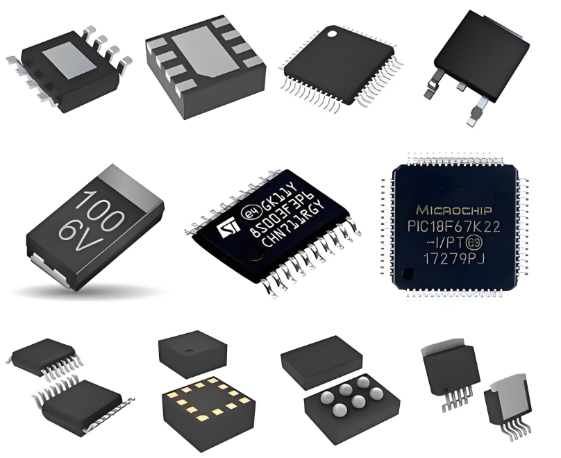
Lattice GAL16V8D-25LPI: An In-Depth Technical Overview of the Classic PLD
In the history of digital logic design, few components have achieved the iconic status of the Lattice GAL16V8. As a specific variant within this renowned family, the GAL16V8D-25LPI stands as a testament to an era where Programmable Logic Devices (PLDs) began to revolutionize electronic system design. This device encapsulates the perfect blend of flexibility, reliability, and cost-effectiveness that made GAL (Generic Array Logic) devices the industry workhorse for decades.
The "GAL16V8" nomenclature is itself descriptive of the chip's capabilities. It indicates a device with a maximum of 16 inputs and 8 outputs, with the internal logic function of each output being user-programmable. The "D" suffix typically denotes a standard commercial temperature range (0°C to 75°C), while "25" specifies a maximum propagation delay of 25 nanoseconds, a respectable speed for a wide range of applications at the time. The "LPI" refers to the package type, in this case, a 20-pin Plastic Leaded Chip Carrier (PLCC), a common surface-mount package that offered a compact footprint.
The heart of the GAL16V8D-25LPI's innovation is its Erasable and Electrically Reprogrammable CMOS technology. Unlike its predecessor, the PAL (Programmable Array Logic), which was one-time programmable (OTP), the GAL device featured a reprogrammable cell based on EECMOS (Electrically Erasable CMOS) technology. This allowed designers to erase and reprogram the device thousands of times, dramatically accelerating the development cycle, debugging, and prototyping processes. This reusability was a monumental leap in productivity.
Architecturally, the device is based on a programmable AND array feeding into fixed OR arrays and sophisticated Output Logic Macro Cells (OLMCs). This is the key to its flexibility. Each of the eight OLMCs can be individually configured by the user into various operational modes, including:
Combinational Output: A simple output derived from the AND-OR array.

Registered Output: An output that passes through a D-type flip-flop, enabling the implementation of sequential logic and state machines.
Combinational I/O: A pin that can act as an input or an output based on the logic function.
Dedicated Input: Configuring an output pin to be an input only.
This configurability meant that a single GAL16V8D-25LPI could replace dozens of standard "7400-series" discrete logic ICs, leading to significant reductions in board space, power consumption, and overall system cost. Its primary applications spanned across glue logic integration, address decoding in microprocessor systems, state machine control, and bus interfacing.
Programming was accomplished using dedicated hardware programmers and software tools like CUPL or Abel, which translated Boolean equations or state diagrams into a JEDEC file. This file was then used to configure the internal fuse map of the device.
While modern FPGAs and CPLDs have far surpassed the GAL16V8 in density and performance, its legacy is undeniable. It served as a critical bridge between rigid discrete logic and the highly flexible programmable logic of today.
ICGOOODFIND: The Lattice GAL16V8D-25LPI is a classic icon in the PLD world, revered for its electrically erasable technology, highly configurable macro cells, and role in consolidating glue logic. It provided a perfect balance of speed, density, and cost for a generation of designs, embodying the shift towards in-system programmability that defines modern electronics.
Keywords: Programmable Logic Device (PLD), Output Logic Macro Cell (OLMC), Electrically Erasable, Glue Logic, JEDEC File
